
Products
Products
8002A
The 8002A is an audio power amplifier for portable electronics. At 5V voltage, the maximum drive power is 1.5W (8Ω load) and 2.0W (4Ω load). The 8002A's application circuit is simple and requires very few peripheral devices.
The 8002A output does not require external coupling capacitors or up-lift capacitors and is packaged in SOP8, making it ideal for low-voltage, low-power audio applications. The 8002A can be controlled into sleep mode to reduce power consumption.
The 8002A output does not require external coupling capacitors or up-lift capacitors and is packaged in SOP8, making it ideal for low-voltage, low-power audio applications. The 8002A can be controlled into sleep mode to reduce power consumption.
8002A Description:
The 8002A is an audio power amplifier for portable electronics. At 5V voltage, the maximum drive power is 1.5W (8Ω load) and 2.0W (4Ω load). The 8002A's application circuit is simple and requires very few peripheral devices.
The 8002A output does not require external coupling capacitors or up-lift capacitors and is packaged in SOP8, making it ideal for low-voltage, low-power audio applications. The 8002A can be controlled into sleep mode to reduce power consumption.
The 8002A eliminates power-on and power-off noise with its innovative "switch/switch noise" suppression technology.
The 8002A operates stably with a gain bandwidth product up to 2.5MHz and a stable unit gain. The voltage gain of the amplifier can be adjusted by configuring the peripheral resistance for easy application.
8002A Features:
No output coupling capacitors or external buffer circuits are required
Stable gain output
External gain setting
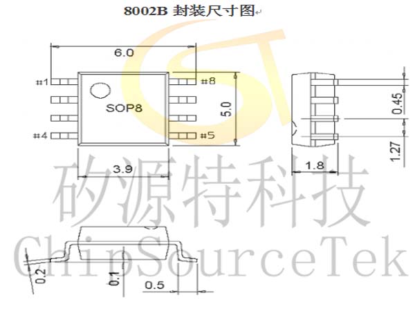
8002A Package: SOP-8
8002A Applications:
Card speaker
Bluetooth speaker
MP3 audio equipment
Portable audio equipment
8002A Typical application circuit diagram:

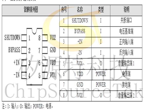
8002A pin diagram and description:
Serial number
| Serial number | name | type | Instructions |
| 1 | SHUTDOWN | I | Turn-off port |
| 2 | BYPASS | I | Voltage reference terminal |
| 3 | +IN | I | Forward input |
| 4 | -IN | I | Reverse input |
| 5 | VO1 | O | Volume output 1 |
| 6 | VDD | POWER | Power terminal |
| 7 | GND | POWER | Ground terminal |
| 8 | VO2 | O | Volume output 2 |
8002A Function Description:
8002A Bridge Configuration:
The 8002A operates internally with 2 amps, the first amps gain can be set externally with RF and RJ resistors (+IN and -IN ports), and the second amps gain is fixed internally. The output signal of the first op amp is actually the input signal of the second op amp, and the signals produced by the two op amps are the same amplitude and opposite phase. Therefore, 8002A gain AVD = 2×(Rf/Ri) is the drive load, and the op amp is set to bridge mode. The bridge mode is different from some common single-ended op-amp circuit output forms to ground one side of the load, and can make the load produce 4 times the output power under the same conditions.
8002A chip power consumption:
Power consumption is one of the key indicators for the amplifier, the maximum self-power consumption of the differential output amplifier is:PDMAX=4×(VDD)2/(2×∏2×RL)
It must be noted that the self-consumption is a function of the output power.
In the circuit design, the internal temperature of the chip cannot be higher than TJMAX (150 ° C), and it is necessary to design according to the thermal resistance of the chip θJA, and the heat dissipation performance can be improved by increasing the heat dissipation copper foil.
If the heat dissipation of the chip still does not meet the requirements, it needs to be solved by increasing the load resistance, reducing the power supply voltage or reducing the ambient temperature. The maximum self-consumption is:
8002A Reference voltage (Bypass terminal voltage)
The external capacitor at the voltage reference end (Bypass) should be as close as possible to 8002A. The 1.0μF capacitor improves the stability of the internal bias voltage and improves the PSRR. The PSRR can be improved by increasing the Bypass capacitance. The actual size depends on the PSRR requirements.
To reduce power consumption, the 8002A's turn-off end (Pin1) can turn off the external bias circuit. When the shutdown end is high (power supply voltage), the op amp is turned off, and the 8002A does not work, then the 8002A operating current is reduced to 4.2uA; When the shutdown end is zero level, the operation amplifier is turned on, and the control pin level of the 8002A shutdown end must be the control signal that meets the requirements of the interface, otherwise the chip may not enter the power failure mode and be in an indeterminate state, and its self-power consumption is not reduced, which cannot achieve the purpose of power saving.
In many applications, the level conversion at the off end is done by the processor. When the one-way knife switch is used to achieve the level conversion, a pull resistance can be added to the off end, so that the level of the 8002A off end is in a stable high level state due to the pull-up resistance, and the op amp remains off.
Selection of 8002A peripheral components
The correct selection of peripheral components can ensure the performance of the chip, although the 8002A has a large margin to guarantee performance, but in order to ensure the overall performance, the correct selection of peripheral components is required.
8002A unit-gain stability (magnification =1), so the use of a wide range, usually use unit-gain amplification to reduce THD+N, and maximize the signal-to-noise ratio, but this requires the input voltage range is large, usually need to make the op amp has a voltage output of 1Vrms.
In addition, the closed-loop bandwidth must also be ensured, and the input coupling capacitance Ci (forming a first-order high-pass) determines the low-frequency response.
8002A Input coupling capacitor
Too large input capacitance will increase the cost and area, which is very bad for cost, area tight applications, it is important to determine how much capacitance to use to complete the input signal coupling. In fact, in many applications, the Speaker cannot reproduce low-frequency speech below 100Hz-150Hz, so the use of large capacitors can not improve the performance of the system.
In addition, the suppression performance of switching/switching noise is affected by the capacitance, if the coupling capacitance is large, the delay of the feedback network is large, resulting in pop noise, so a small coupling capacitance can reduce the noise.
In addition, you must consider the size of the Bypass capacitor. Select CBy=1uF and Ci = 0.1uF ~ 0.39uF to meet the system performance.
8002A Limit parameter (Ta=25℃)
| peculiarity | symbol | Minimum value | Maximum value | unit |
| Supply voltage | VDD | - | 7 | V |
| Operating temperature | TOPR | -40 | 85 | ℃ |
| 环Ambient temperature | TA | -65 | 150 | ℃ |
| Node temperature | TJ | 150 | ℃ | |
| HBM ESD pressure resistant | 2000 | |||
| MM ESD Withstand high pressure | 200 |
8002A Electrical specifications(VDD=5V,RL=8Ω,Ta=25℃)
| argument | symbol | Test condition | Minimum value | Standard value | Maximum valueunit | |
| Static current of supply | IDD | VIN=0V,IO=0A, no load | 4.4 | mA | ||
| VIN=0V,IO=0A, load 8Ω | 4.3 | |||||
| Operating voltage | VDD | 1.6 | 6 | V | ||
| Chip power leakage current | IOFF | 4.2 | uA | |||
| Output offset voltage | VOS | 3.7 | 20 | mV | ||
| Output resistance | RO | 7 | 8.5 | 10 | KΩ | |
| Output power 8Ω | PO | THD+N<1%,f=1KHZ | 1.1 | W | ||
| THD+N<10%,f=1KHZ | 1.6 | W | ||||
| Output power 4Ω | THD+N<1%,f=1KHZ | 1.6 | W | |||
| THD+N<10%,f=1KHZ | 2.4 | W | ||||
| Chip wake up time | TD | 100 | ms | |||
| Total harmonic + distortion noise | THD+N | PO=0.5Wrms;f=1KHZ | 0.1 | 0.2 | % | |
| Power supply voltage rejection ratio | PSRR | Vripple=200mVPP,Sine wave, input connected to 10Ω resistor | 60 | 63@f=217Hz 68@f=1KHz | dB |
8002A package diagram:

Please submit your basic information, send an email to Sales@ChipSourceTek.com, or call us at 13823761625 (same number as WeChat), and we will contact you as soon as possible!

WeChat Official Account

WeChat Service
 Email
Email QQ
QQ 13823761625
