
Products

SC8002B
When operating at 5V input voltage, the average power on the load (3Ω) is 3W, and the distortion does not exceed 10%. For portable devices, when the VDD is applied to the turn-off end, the SC8002B will enter the turn-off mode, and the power consumption at this time is extremely low, and the IQ is only 0.6uA. The SC8002B is an audio amplifier IC designed for high-power, high-fidelity applications. It requires few peripheral components and can work at an input voltage of 2.0V ~ 5.5V.
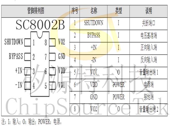
The SC8002B is an audio power amplifier IC with turn-off mode.
When operating at 5V input voltage, the average power on the load (3Ω) is 3W, and the distortion does not exceed 10%. For portable devices, when the VDD is applied to the turn-off end, the SC8002B will enter the turn-off mode, and the power consumption at this time is extremely low, and the IQ is only 0.6uA.
The SC8002B is an audio amplifier IC designed for high-power, high-fidelity applications. It requires few peripheral components and can work at an input voltage of 2.0V ~ 5.5V.
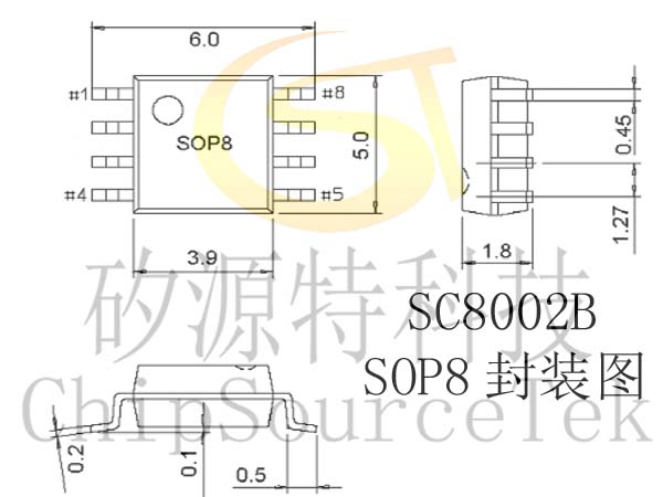
The SC8002B offers a SOP8 package.
Stable gain output.
External gain setting
The SC8002B is available in a SOP8 package
PDMAX = (TJMAX-TA)/ θJA
Note: SOP package θJA=140°C/W, DIP package θJA=107°C/W, MSOP package θJA=210°C/W
In many applications, the level conversion at the off end is done by the processor. When the unidirectional knife switch is used to achieve the level conversion, a pull resistor can be added to the off end, so that when the switch is off, the level of the SC8002B off end will be in a correct state due to the pull up resistance, so as to ensure that the SC8002B will not enter the wrong working state.
SC8002B limit parameter (Ta=25℃):
peculiarity | symbol | Radius | unit |
Operating voltage | VDD | 6 | V |
Input voltage | VIN | -0.3~VDD+0.3 | V |
Operating temperature | TOPR | -65~+150 | ℃ |
Ambient temperature | TA | -40~+85 | ℃ |
Node temperature | TJ | 150 | ℃ |
SC8002B: Electrical parameters(VDD=5V,RL=8Ω,Ta=25℃)
name | symbol | Minimum value | Typical value | Maximum value | unit | Test condition |
Operating voltage | VDD | 2.0 | -- | 5.5 | V | |
Static current | IDD | -- | 6.5 | 10 | mA | VIN=0V, IO=0mA |
Turn-off current | ISD | -- | 0.6 | 2 | uA | VPIN1=VDD |
Output bias | VOS | -- | 5.0 | 50 | mV | VIN=0V |
Output power | PO | -- | 1.2 | -- | W | THD=1%, f=1KHz, RL=8Ω |
-- | 1.5 | -- | THD=10%, f=1KHz,RL=8Ω | |||
Total harmonic distortion + noise | THD+N | -- | 0.25 | -- | % | 20Hz≤f≤20KHz, AVD=2, RL=8Ω, PO=1W |
Power supply rejection ratio | -- | 60 | -- | dB | VDD=4.9V~5.1V |
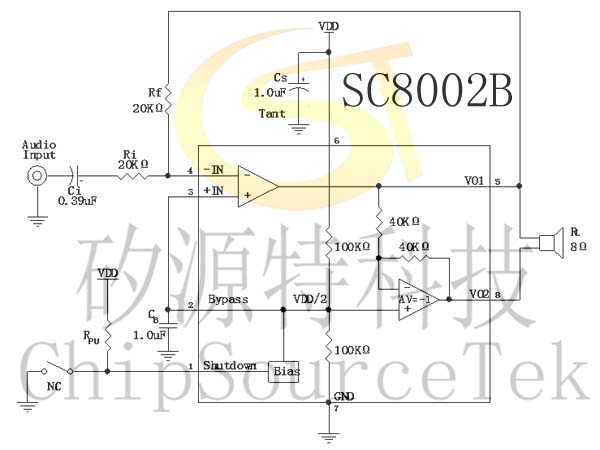
SC8002B circuit schematic diagram:

Please submit your basic information, send an email to Sales@ChipSourceTek.com, or call us at 13823761625 (same number as WeChat), and we will contact you as soon as possible!

WeChat Official Account

WeChat Service
 Email
Email QQ
QQ 13823761625
