
Products
Products

TC8871
The TC8871 is an FM free, Class AB /D optional power amplifier.
When the operating voltage is 5V, the maximum driving power is 5W (2? , BTL load, THD<10%), TC8871 has an internal overheat automatic shutdown protection mechanism; Stable operation, gain bandwidth product up to 2.5MHz, and unit gain stability.
The TC8871 is the perfect solution for your USB subwoofer and amplifier.
TC8871 Description:
The TC8871 is an FM free, Class AB /D optional power amplifier.
When the operating voltage is 5V, the maximum driving power is 5W (2? , BTL load, THD<10%), the total harmonic distortion noise in the audio range is less than 1%.
TC8871 application circuit is simple, only a few peripheral devices, integrated feedback resistance; The output does not require external coupling capacitors or up-lift capacitors and buffering networks. The TC8871 is packaged in an ESOP package and is particularly suitable for use in portable systems with low volume and weight. Sleep mode can be controlled to reduce power consumption.
The TC8871 has an automatic overheat shutdown protection mechanism inside; Stable operation, gain bandwidth product up to 2.5MHz, and unit gain stability. The feedback resistance is built in, and the voltage gain and sound quality of the amplifier can be adjusted by configuring peripheral parameters, which is convenient for application.
The TC8871 is the perfect solution for your USB subwoofer and amplifier.
TC8871 Feature:
No interference to FM, high efficiency, sound quality
High output power (THD+N<10%, 1KHz frequency)
The ESOP package is 5W (2? Load) and 3.5W (3? Load), 3W (4? Load)
Power failure mode leakage current is small
The TC8871 is packaged in ESOP
Adjustable external gain, integrated feedback
Wide operating voltage range 2.0V~5.0V
There is no need to drive output coupling capacitors, bootstrap capacitors and buffer networks
Unit gain stabilization
Compatible with 4871, 8002 series, 6871, 5128, 2018, etc
TC8871 Application:
megaphone
Apply portable speakers/card speakers
Apply Bluetooth speaker/USB speaker
Apply portable speakers/card speakers
Apply Bluetooth speaker/USB speaker
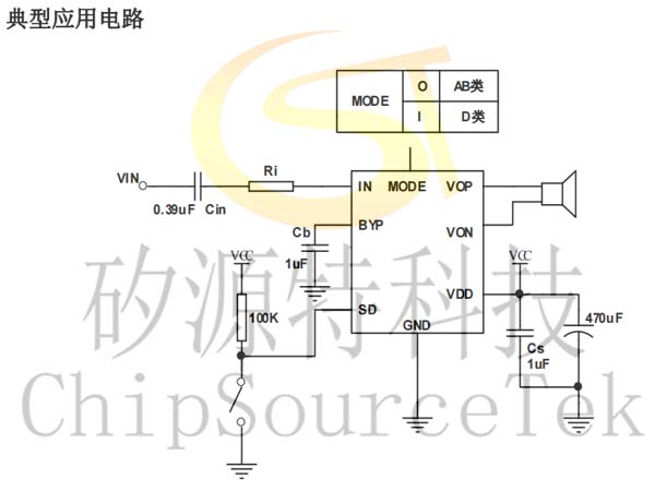
TC8871 application circuit diagram:
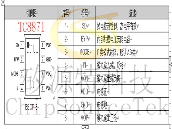
TC8871 pin diagram and pin description:
TC8871 Limiting parameter
TC8871 Electrical parameter
TC8871 Class D mode application description
TC8871 MODE function
The TC8871 is a Class AB/Class D optional audio power amplifier, which can be selected by the MODE function key.
TC8871 Input Resistance (Ri)
The gain of the amplifier can be configured by selecting the parameter values of the input resistance:
1 Decoupling capacitor
The TC8871 is a high-performance Class D audio power amplifier that requires proper power decoupling to ensure its high efficiency and low harmonic distortion. The decoupling capacitor uses a low-impedance ceramic capacitor with a capacity of 1uf, as close as possible to the chip power supply power supply pin, because any resistance, capacitance and inductance in the circuit can affect the efficiency of the power conversion. A capacitor of 10uf or larger placed near the amplifier will provide better filtering results, but such a capacitor is not required in amplifier applications with high supply voltage rejection coefficients.
TC8871 Input capacitance
If the differential input signal in the design is in the range of 0.5V to VCC-0.8V, if the input signal amplitude is not in this range, the input is a high-pass filter or 8871 used in a single-ended input system, the input capacitance is required. When the input is used as a high-pass filter, the calculation formula of the filter center frequency is as follows:
(2)
The parameters of input resistance and input capacitance directly affect the lower frequency of the filter and thus the performance of the amplifier. The input capacitance is calculated as follows:
(3)
If the input frequency of the signal is in the audio range, the accuracy of the input capacitance can be ± 10% or higher, because capacitor mismatches can affect the performance of the filter. Using large capacitance (1uf) can reproduce low frequency signal very well. But in GSM phones, the ground signal wobbles up and down at 217Hz, but there is no such wobble in the signal of the multimedia digital signal decoder.
TC8871 output filter
When using the 8871 without an output filter, the length of the connection from the amplifier to the speaker is generally less than 100mm. In portable communication devices such as mobile phones, the PAD can be used without output filters. In some environmental and other conditions do not allow and some special cases, to add the output filter, add a low-pass filter, such as LC filter
Typical application circuit of the output patch ferrite magnetic bead filter
Output plus LC filter Typical application circuit (cut-off frequency is 27KHz)
Overview of the TC8871 protection function mode
The 8871 is a crack-free Class D audio power amplifier. And built-in overcurrent protection, overheat protection and undervoltage protection and other functions. Effectively protect the chip from being damaged under abnormal working conditions. The 8871 goes into overcurrent protection mode. The mode can be cancelled after the power is switched on and off again.
TC8871 Class AB mode application description
The TC8871 is integrated with two operational amplifiers, the gain of the first amplifier can be set by adjusting the feedback resistance, and the latter is the inverse voltage to follow, thus forming an amplifier drive circuit with a differential output whose gain can be configured.
TC8871 External resistance configuration
As shown in the application diagram, the gain of the operational amplifier is determined by the external resistance Rf and Ri, and its gain is Av=2×Rf/Ri, and the chip is output to the load through VO1 and VO2.
The bridge connection has several advantages over the single-ended output: first, it eliminates the need for external straight filter capacitance. Single-end output, if no direct capacitor is connected, there is a constant current voltage at the output end, resulting in DC current output after power-on, which wastes power consumption and is easy to damage the sound. The second is that the double-ended output is actually the push-pull output, and under the same output voltage, the drive power is increased to 4 times that of the single end, and the power output is large.
TC8871 chip power consumption
Power consumption is one of the key indicators for the amplifier, the maximum self-power consumption of the differential output amplifier is:
PDMAX = 4× (VDD) 2/ (2×π2×RL)
It must be noted that the self-consumption is a function of the output power.
In the circuit design, the internal temperature of the chip can not be higher than TJMAX (150oC), according to the thermal resistance of the chip. JA to design, you can increase the heat dissipation performance by cooling copper platinum itself.
If the chip still does not meet the requirements, it is necessary to increase the load resistance, reduce the power supply voltage or reduce the ambient temperature to solve the problem.
TC8871 Power bypass
In the application of amplifier, the bypass design of the power supply is very important, especially for the noise performance of the application scheme and the power supply voltage suppression performance. In the design, the bypass capacitor is required to be as close to the chip and power pin as possible. The typical capacitance is a 10uF electrolytic capacitor and a 0.1uF ceramic capacitor.
In the 8871 application circuit, the other capacitor CB (with BYP pin) is also very critical, affecting PSRR, switching/switching noise performance. Generally choose 0.1uF ~ 1uF ceramic capacitor.
TC8871 Power failure mode
In order to save power, the amplifier can be turned off when not in use, and the 8871 has a power down control pin to control whether the amplifier works.
The level of the control pin must be connected to the control signal that meets the requirements of the interface, otherwise the chip may enter the uncertain state, but can not enter the power failure mode, and its self-power consumption is not reduced, which cannot achieve the purpose of power saving.
TC8871 Select input coupling capacitor
Too large input capacitance increases the cost and increases the area, which is very unfavorable for applications where the cost and area are tight. Obviously, it is important to determine how much capacitance to use to complete the coupling. In fact, in many applications, the Speaker cannot reproduce low-frequency speech below 100Hz-150Hz, so the use of large capacitors can not improve the performance of the system.
In addition to considering the performance of the system, the suppression performance of switching/switching noise is affected by the capacitance, if the coupling capacitance is large, the delay of the feedback network is large, resulting in pop noise, so a small coupling capacitance can reduce the noise.
In addition, the size of CB capacitance must be considered, CB=1μF, Ci = 0.1μF ~ 0.39μF, can meet the performance of the system.
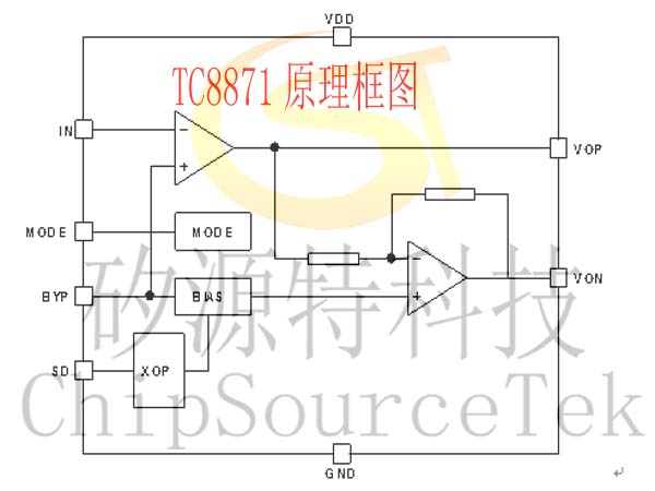
TC887 block diagram:
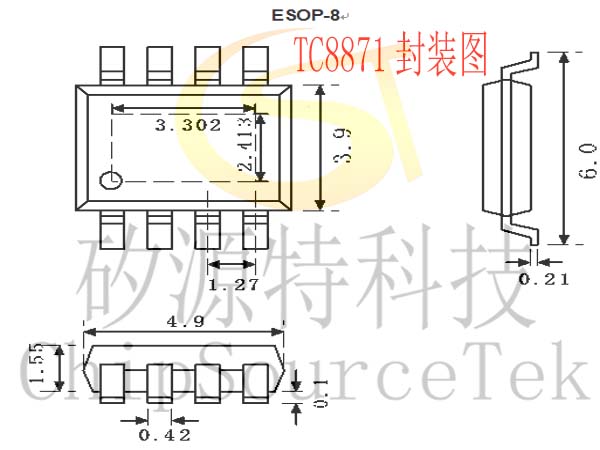
TC8871 package diagram:
TC8871 Limiting parameter
| argument | Minimum value | Maximum value | unit | Instructions |
|---|---|---|---|---|
| Supply voltage | 1.8 | 6 | V | |
| Storage temperature | -65 | 150 | oC | |
| Input voltage | -0.3 | VDD | V | |
| ESD voltage resistance 1 | 3000 | V | HBM | |
| ESD voltage resistance 2 | 250 | V | MM | |
| Temperature saving | 150 | oC | Typical value 150 | |
| Recommended operating temperature | -40 | 85 | oC | |
| Recommended operating voltage | 2.0 | 5.5 | ||
| Thermal resistance | ||||
| ?JC(SOP) | 35 | oC/W | ||
| ?JA(SOP) | 140 | oC/W | ||
| ?JC(LLP) | 4.3 | oC/W | ||
| ?JA(LLP) | 56 | oC/W | ||
| Welding temperature | 220 | oC | In 15 seconds | |
TC8871 Electrical parameter
| symbol | argument | Test condition | Minimum value | Standard value | Maximum value | unit |
|---|---|---|---|---|---|---|
| VDD | Supply voltage | 2.0 | 5.5 | V | ||
| IDD | Static current of supply | VIN=0V,IO=0A, | 6 | 10 | mA | |
| ISD | Turn off the leakage current | 0.8 | 2 | µA | ||
| VOS | Output offset voltage | 5.7 | 50 | mV | ||
| RO | Output resistance | 7 | 8.5 | 10 | K? | |
| PO | Output power | THD=1%,f=1KHz,RL=4Ω | 2 | W | ||
| THD+N=10%,f=1KHz,RL=4Ω | 3 | W | ||||
| THD+N | Total distortion + noise | AVD=2,20Hz≤f≤20KHz RL=4Ω,PO=0.5W | 0.2 | % | ||
| PSRR | Power supply rejection ratio | VDD=4.9V到5.1V | 65 | 80 | dB |
TC8871 Class D mode application description
TC8871 MODE function
The TC8871 is a Class AB/Class D optional audio power amplifier, which can be selected by the MODE function key.
| MODE | Chip function mode |
| High level | Class D power amplifier |
| Low level | Class AB power amplifier |
The gain of the amplifier can be configured by selecting the parameter values of the input resistance:
1 Decoupling capacitor
The TC8871 is a high-performance Class D audio power amplifier that requires proper power decoupling to ensure its high efficiency and low harmonic distortion. The decoupling capacitor uses a low-impedance ceramic capacitor with a capacity of 1uf, as close as possible to the chip power supply power supply pin, because any resistance, capacitance and inductance in the circuit can affect the efficiency of the power conversion. A capacitor of 10uf or larger placed near the amplifier will provide better filtering results, but such a capacitor is not required in amplifier applications with high supply voltage rejection coefficients.
TC8871 Input capacitance
If the differential input signal in the design is in the range of 0.5V to VCC-0.8V, if the input signal amplitude is not in this range, the input is a high-pass filter or 8871 used in a single-ended input system, the input capacitance is required. When the input is used as a high-pass filter, the calculation formula of the filter center frequency is as follows:
(2)
The parameters of input resistance and input capacitance directly affect the lower frequency of the filter and thus the performance of the amplifier. The input capacitance is calculated as follows:
(3)
If the input frequency of the signal is in the audio range, the accuracy of the input capacitance can be ± 10% or higher, because capacitor mismatches can affect the performance of the filter. Using large capacitance (1uf) can reproduce low frequency signal very well. But in GSM phones, the ground signal wobbles up and down at 217Hz, but there is no such wobble in the signal of the multimedia digital signal decoder.
TC8871 output filter
When using the 8871 without an output filter, the length of the connection from the amplifier to the speaker is generally less than 100mm. In portable communication devices such as mobile phones, the PAD can be used without output filters. In some environmental and other conditions do not allow and some special cases, to add the output filter, add a low-pass filter, such as LC filter
Typical application circuit of the output patch ferrite magnetic bead filter
Output plus LC filter Typical application circuit (cut-off frequency is 27KHz)
Overview of the TC8871 protection function mode
The 8871 is a crack-free Class D audio power amplifier. And built-in overcurrent protection, overheat protection and undervoltage protection and other functions. Effectively protect the chip from being damaged under abnormal working conditions. The 8871 goes into overcurrent protection mode. The mode can be cancelled after the power is switched on and off again.
TC8871 Class AB mode application description
The TC8871 is integrated with two operational amplifiers, the gain of the first amplifier can be set by adjusting the feedback resistance, and the latter is the inverse voltage to follow, thus forming an amplifier drive circuit with a differential output whose gain can be configured.
TC8871 External resistance configuration
As shown in the application diagram, the gain of the operational amplifier is determined by the external resistance Rf and Ri, and its gain is Av=2×Rf/Ri, and the chip is output to the load through VO1 and VO2.
The bridge connection has several advantages over the single-ended output: first, it eliminates the need for external straight filter capacitance. Single-end output, if no direct capacitor is connected, there is a constant current voltage at the output end, resulting in DC current output after power-on, which wastes power consumption and is easy to damage the sound. The second is that the double-ended output is actually the push-pull output, and under the same output voltage, the drive power is increased to 4 times that of the single end, and the power output is large.
TC8871 chip power consumption
Power consumption is one of the key indicators for the amplifier, the maximum self-power consumption of the differential output amplifier is:
PDMAX = 4× (VDD) 2/ (2×π2×RL)
It must be noted that the self-consumption is a function of the output power.
In the circuit design, the internal temperature of the chip can not be higher than TJMAX (150oC), according to the thermal resistance of the chip. JA to design, you can increase the heat dissipation performance by cooling copper platinum itself.
If the chip still does not meet the requirements, it is necessary to increase the load resistance, reduce the power supply voltage or reduce the ambient temperature to solve the problem.
TC8871 Power bypass
In the application of amplifier, the bypass design of the power supply is very important, especially for the noise performance of the application scheme and the power supply voltage suppression performance. In the design, the bypass capacitor is required to be as close to the chip and power pin as possible. The typical capacitance is a 10uF electrolytic capacitor and a 0.1uF ceramic capacitor.
In the 8871 application circuit, the other capacitor CB (with BYP pin) is also very critical, affecting PSRR, switching/switching noise performance. Generally choose 0.1uF ~ 1uF ceramic capacitor.
TC8871 Power failure mode
In order to save power, the amplifier can be turned off when not in use, and the 8871 has a power down control pin to control whether the amplifier works.
The level of the control pin must be connected to the control signal that meets the requirements of the interface, otherwise the chip may enter the uncertain state, but can not enter the power failure mode, and its self-power consumption is not reduced, which cannot achieve the purpose of power saving.
TC8871 Select input coupling capacitor
Too large input capacitance increases the cost and increases the area, which is very unfavorable for applications where the cost and area are tight. Obviously, it is important to determine how much capacitance to use to complete the coupling. In fact, in many applications, the Speaker cannot reproduce low-frequency speech below 100Hz-150Hz, so the use of large capacitors can not improve the performance of the system.
In addition to considering the performance of the system, the suppression performance of switching/switching noise is affected by the capacitance, if the coupling capacitance is large, the delay of the feedback network is large, resulting in pop noise, so a small coupling capacitance can reduce the noise.
In addition, the size of CB capacitance must be considered, CB=1μF, Ci = 0.1μF ~ 0.39μF, can meet the performance of the system.
TC887 block diagram:
TC8871 package diagram:

Please submit your basic information, send an email to Sales@ChipSourceTek.com, or call us at 13823761625 (same number as WeChat), and we will contact you as soon as possible!

WeChat Official Account

WeChat Service
 Email
Email QQ
QQ 13823761625
