
Products
Products


OPA1612-8002D
The OPA1612-8002D is an audio power amplifier IC with turn-off mode. When operating at 5V input voltage, the average power on the load (3Ω) is 3W, and the distortion does not exceed 10%. For portable devices, when VDD is applied to the turn-off end, the OPA1612-8002D will enter the turn-off mode, and the power consumption is extremely low.
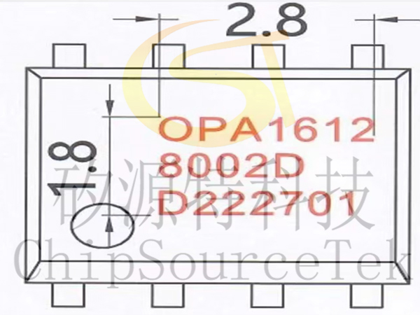
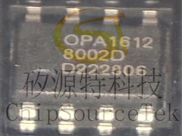
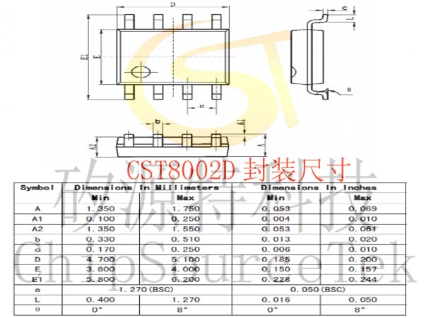
The OPA1612-8002D is packaged with SOP8.
The OPA1612-8002D is packaged with SOP8.
OPA1612-8002D Description:
VDD=5V,RL=3Ω,Po=3W,THD+N≤10%
Wide operating voltage range 1.8V - 5.5V
Excellent on-off POP acoustic suppression
No output coupling capacitors, bootstrap capacitors and buffering networks are required
Unit gain stabilization
The OPA1612-8002D is packaged in SOP8
Excellent on-off POP acoustic suppression
No output coupling capacitors, bootstrap capacitors and buffering networks are required
Unit gain stabilization
The OPA1612-8002D is packaged in SOP8
Sound toy
Security monitoring system
Low voltage sound system
Bluetooth speaker
Security monitoring system
Low voltage sound system
Bluetooth speaker
Chip type | Package type | Packaging type | Minimum packing quantity (PCS) |
SOP8 | piping | 100/ tube | |
SOP8 | Disk mounting | 4000/Disk |

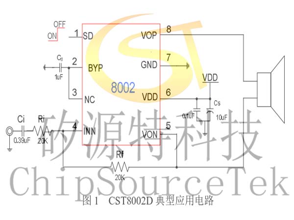
Note: The components in the above application diagram are described:
Ci: Straight capacitance, 0.39µF or less, further eliminates clatter-pitting and noise coupled in from the input.
Cs: Power decoupling capacitor, use a sufficiently low ESR capacitor (less than 1µF), when VDD=5V, it is recommended to add another low ESR capacitor (not less than 10µF) to better filter out low frequency noise. The closer the decoupling capacitor is to the VDD pin, the better. Keep it within 1.5mm.
CB: The BYPASS port outputs VDD/2 voltage and is grounded through a capacitor CB (1µF) to ensure stability.
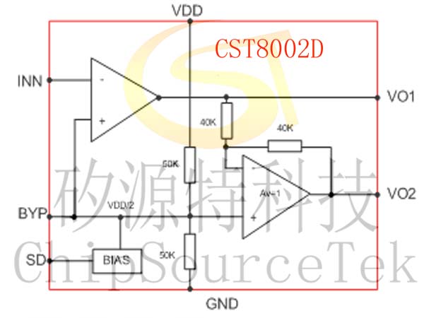
OPA1612-8002D引脚分布图:
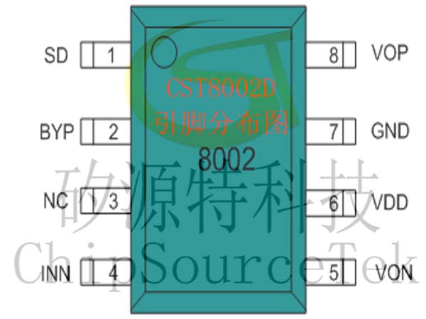
OPA1612-8002D管脚描述:
管脚号 | 符号 | 描述 |
1 | SD | 关断控制端,高电平关断 |
2 | BYP | 偏置电压输出端 |
3 | NC | 无连接,芯片内部连接至BYP |
4 | INN | 负相输入端 |
5 | VON | 负相输出端 |
6 | VDD | 电源 |
7 | GND | 地 |
8 | VOP | 正相输出端 |

Please submit your basic information, send an email to Sales@ChipSourceTek.com, or call us at 13823761625 (same number as WeChat), and we will contact you as soon as possible!

WeChat Official Account

WeChat Service
 Email
Email QQ
QQ 13823761625
