
Products
Products

LTK5313
The LTK5313 is a built-in adaptive boost Class F audio power amplifier chip with AGC anti-crack function, AB/D class mode switching, adaptive, ultra-low background noise, ultra-low EMI. When the output amplitude is small, the booster circuit does not work, and the power amplifier is directly powered by the power supply. When the output is large, the internal booster circuit automatically starts, and the power amplifier supply voltage is the boost voltage to achieve greater output power. The LTK5313 is available in four AGC modes to meet a wide range of needs and protect speakers from overload damage.
The LTK5313 has a Class AB/D switching function, which can reduce the FM interference of the power amplifier in class AB. The fully differential structure effectively improves the power amplifier's RF noise suppression. Charge Pump
The LTK5313 has a Class AB/D switching function, which can reduce the FM interference of the power amplifier in class AB. The fully differential structure effectively improves the power amplifier's RF noise suppression. Charge Pump
LTK5313 Description:
The LTK5313 is a built-in adaptive boost Class F audio power amplifier chip with AGC anti-crack function, AB/D class mode switching, adaptive, ultra-low background noise, ultra-low EMI. When the output amplitude is small, the booster circuit does not work, and the power amplifier is directly powered by the power supply. When the output is large, the internal booster circuit automatically starts, and the power amplifier supply voltage is the boost voltage to achieve greater output power.
The LTK5313 is available in four AGC modes to meet a wide range of needs and protect speakers from overload damage. The chip has the AB/D class switching function, which can reduce the FM interference when the power amplifier is in class AB. The fully differential structure effectively improves the power amplifier's RF noise suppression. Charge Pump boost mode, no external inductor, Schottky diode, to reduce peripheral components as much as possible, save costs.
The LTK5313 is available in four AGC modes to meet a wide range of needs and protect speakers from overload damage. The chip has the AB/D class switching function, which can reduce the FM interference when the power amplifier is in class AB. The fully differential structure effectively improves the power amplifier's RF noise suppression. Charge Pump boost mode, no external inductor, Schottky diode, to reduce peripheral components as much as possible, save costs.
LTK5313 Feature:
Input voltage range 2.8V-5.5V
Four types of automatic Gain Control (AGC)
One line pulse control chip working mode
The built-in adaptive Charge Pump boost automatically increases the voltage to 6.5V
No filter Class D amplifier, low static current and low EMI
Excellent burst suppression circuit
Ultra-low bottom noise, ultra-low distortion
10%THD+N, VDD=4.2V, delivers up to 5W of output power under 4Ω+33UH load
1%THD+N, VDD=4.2V, delivers up to 4.2W of output power at 4Ω +33UH loads
Short circuit protection, under voltage protection, over temperature protection
Turn-off current < 1ua
Bluetooth speaker, smart speaker
Navigator, portable game console
Pull rod speaker, DVD, amp, MP3, MP4
Smart home and other audio products
Navigator, portable game console
Pull rod speaker, DVD, amp, MP3, MP4
Smart home and other audio products
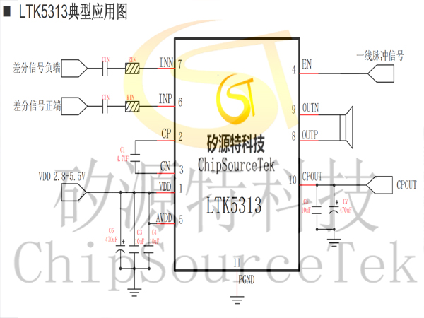
At the CPOUT end, 470UF or 1000uf plug-in capacitor and 10UF ceramic capacitor are selected in parallel according to the load, and the capacitor is as close as possible to the CPOUT pin. The VDD end also uses the 470UFV plug-in capacitor and the 10UF ceramic capacitor in parallel.
Power supply foot (VDD, CPOUT) wiring as thick as possible, it is best to use copper to connect the network, such as wiring or copper must be drilled in the hole should use porous connection, and increase the hole diameter, can not use a single hole directly connected to the power line, because the large current will cause a large voltage drop, will lead to a larger voltage drop, the output power has a greater impact, If there is a large impedance in the power supply and even affect the sound, there will be a stuttering situation.
Input capacitance (Cin) and input resistance (Rin) are placed as close as possible to the pin of the power amplifier chip, and it is best to use the ground routing mode, which can effectively suppress the noise of other signal coupling.
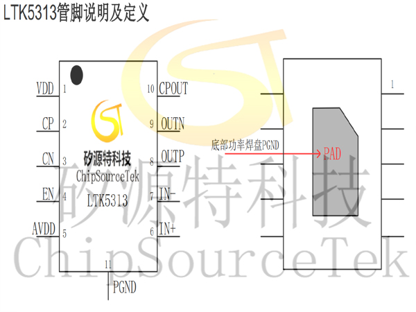
The bottom heat sink of LTK5313 is the only ground point of the chip and must be connected to the PCB board. When designing the PCB, the bottom window must be opened and the GND connection with the chip and PCB is used, which is of great help to the heat dissipation of the chip. The PCB uses a large area of copper to connect the heat sink in the middle of the chip and has a certain range of copper exposure. The pin of the LTK5313 output connected to the horn should be as short as possible, and the width of the cable should be at least 0.4mm.
Power supply foot (VDD, CPOUT) wiring as thick as possible, it is best to use copper to connect the network, such as wiring or copper must be drilled in the hole should use porous connection, and increase the hole diameter, can not use a single hole directly connected to the power line, because the large current will cause a large voltage drop, will lead to a larger voltage drop, the output power has a greater impact, If there is a large impedance in the power supply and even affect the sound, there will be a stuttering situation.
Input capacitance (Cin) and input resistance (Rin) are placed as close as possible to the pin of the power amplifier chip, and it is best to use the ground routing mode, which can effectively suppress the noise of other signal coupling.
The bottom heat sink of LTK5313 is the only ground point of the chip and must be connected to the PCB board. When designing the PCB, the bottom window must be opened and the GND connection with the chip and PCB is used, which is of great help to the heat dissipation of the chip. The PCB uses a large area of copper to connect the heat sink in the middle of the chip and has a certain range of copper exposure. The pin of the LTK5313 output connected to the horn should be as short as possible, and the width of the cable should be at least 0.4mm.
If the actual power test is different from the specifications, it is recommended to check whether the PCB power supply cable is thick enough, whether the contact impedance is too large, whether the power supply current is sufficient, whether the power supply voltage drop exists, and whether the component current is insufficient.
When the play is stuck, check the discharge capacity of the battery, replace the battery with a larger current, check the impedance and components of the system according to the above check items, check whether the capacitor is placed too far away, and check whether there is a single throughhole in the GND of the large current and large current path.
FM radio station less: Check whether the power amplifier chip is switched to class AB mode, and use the oscilloscope to measure the output to confirm the working status.
When the POPO tone is large: Use the oscilloscope to check whether the timing of the main control MUTE is correct.
If the EN switching mode fails to enter the corresponding mode, check whether the pulse signal meets the requirements.

Please submit your basic information, send an email to Sales@ChipSourceTek.com, or call us at 13823761625 (same number as WeChat), and we will contact you as soon as possible!

WeChat Official Account

WeChat Service
 Email
Email QQ
QQ 13823761625
