
Products
Products

LTK4871
The LTK4871 is a 3W, mono Class AB audio power amplifier chip. Operating voltage 2V-5V, in the way of BTL bridge connection, under 5V supply voltage, can provide a 4Ω load THD less than 10%, the average output power of 3.0W. In off mode, the current is typically less than 0.5uA.
The LTK4871 is designed to provide high-power, high-fidelity audio output, requiring only a few peripherals and operating at low voltage conditions (2V-5V).
The LTK4871 does not require coupling capacitors, bootstrap capacitors, or buffering networks, making it ideal for low-power systems with small volumes.
The LTK4871 is available in an ESOP-8 package
LTK4871 Description:
The LTK4871 is a 3W, mono Class AB audio power amplifier chip. Operating voltage 2V-5V, in the way of BTL bridge connection, under 5V supply voltage, can provide a 4Ω load THD less than 10%, the average output power of 3.0W. In off mode, the current is typically less than 0.5uA.
The LTK4871 is designed to provide high-power, high-fidelity audio output, requiring only a few peripherals and operating at low voltage conditions (2V-5V).
The LTK4871 does not require coupling capacitors, bootstrap capacitors, or buffering networks, making it ideal for low-power systems with small volumes.
The LTK4871 is available in an ESOP-8 package
The LTK4871 is designed to provide high-power, high-fidelity audio output, requiring only a few peripherals and operating at low voltage conditions (2V-5V).
The LTK4871 does not require coupling capacitors, bootstrap capacitors, or buffering networks, making it ideal for low-power systems with small volumes.
The LTK4871 is available in an ESOP-8 package
LTK4871 Features:
Built-in switching noise suppression circuit
10% THD+N, VDD=5V, 4Ω load, provides up to 3W output power
10% THD+N, VDD=5V, 8Ω load, provides up to 1.8W output power
Turn-off current < 0.5uA
The LTK4871 is available in an ESOP-8 package
Overheat protection
10% THD+N, VDD=5V, 4Ω load, provides up to 3W output power
10% THD+N, VDD=5V, 8Ω load, provides up to 1.8W output power
Turn-off current < 0.5uA
The LTK4871 is available in an ESOP-8 package
Overheat protection
LTK4871 Applications:
Cassette speaker
Bluetooth speaker
Lithium megaphone
FM player
Bluetooth speaker
Lithium megaphone
FM player
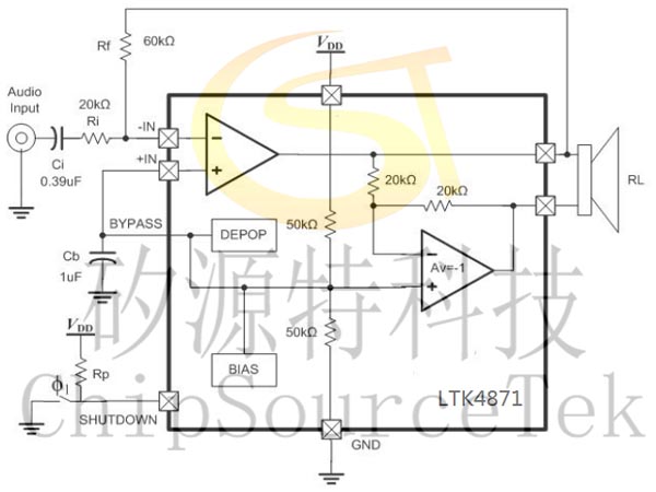
LTK4871 Typical application circuit:
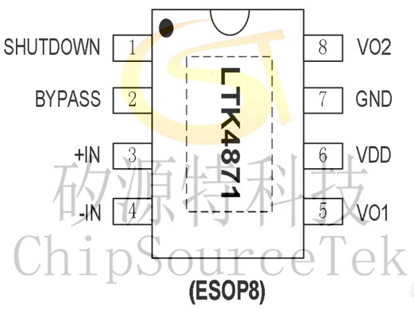
LTK4871 power amplifier circuit pin map:
LTK4871 Package Information:
| product | Encapsulation form | Package size (mm) | Distance between feet (mm) |
| LTK4871 | ESOP-8 |
LTK4871 Max rating (TA=25℃)
| Parameter name | symbol | Numerical value | unit |
| Operating voltage | Vcc | 6.0 | V |
| Storage temperature | Tstg | -65℃-150℃ | ℃ |
| Input voltage | -0.3 to +(0.3+ Vcc) | V | |
| Power consumption | PD | See note 1 | W |
| Junction temperature | 160℃ | ℃ |
LTK4871 Pin Description:
| No. | Pin name | IO | Work and energy |
| 1 | SHUTDOWN | I | Off mode control input, high power normally off. |
| 2 | BYPASS | I | The voltage is VDD/2 and the external capacitor is connected. |
| 3 | IN+ | I | IN+ is the forward input end. IN+ is usually connected to the Bypass Pin. |
| 4 | IN- | I | IN- is a negative input, used for audio input. |
| 5 | VO+ | I | VO+ is the forward output of BTL. |
| 6 | VDD | - | Power input |
| 7 | GND | - | electrically |
| 8 | VO- | O | VO- is the negative output of BTL. |
LTK4871 Electrical parameters:
Electrical parameter
VDD=5V, TA=25℃
| signal | Parameter name | Test condition | Minimum value | Typical value | Maximum value | unit |
| VDD | Supply voltage | 5 | V | |||
| IDD | Static supply current | VDD=5V,IO=0A | 5.5 | 7.5 | 9.5 | mA |
| ISHDN | Turn-off current | VDD=2V 到 5.5V | 0.5 | uA | ||
| Po | output power | THD+N=10%, f=1kHz ,RL=4Ω; | 3 | W | ||
| THD+N=10%, f=1kHz,RL=3Ω; | 3.4 | |||||
| THD+N=10%, f=1kHz,RL=8Ω; | 1.8 | |||||
| THD+N=1%, f=1kHz ,RL=4Ω; | 2.3 | |||||
| THD+N=1%, f=1kHz ,RL=3Ω; | 2.5 | |||||
| THD+N=1%, f=1kHz ,RL=8Ω; | 1.3 | |||||
| THD+N | Total harmonic distortion plus noise | VDD=5V Po=0.6W, RL=8Ω | 0.1 | % | ||
| VDD=5V Po=1.6W, RL=4Ω | 0.15 | |||||
| OTP | Overtemperature protection | 165 | ℃ | |||
| PSRR | Power supply voltage rejection ratio | VDD=5V, VRIPPLE=200mVRMS, RL=8Ω, CB=2.2µF | 70 | dB |

Please submit your basic information, send an email to Sales@ChipSourceTek.com, or call us at 13823761625 (same number as WeChat), and we will contact you as soon as possible!

WeChat Official Account

WeChat Service
 Email
Email QQ
QQ 13823761625
