
Products
Products
LTK5127
The LTK5127 is a 5W, mono Class AB/Class D mode switching, ultra-low EMI, no filter audio power amplifier chip.
The LTK5127 can be easily switched to Class AB MODE through a mode pin, completely eliminating EMI interference. Operating voltage of 2.5V-5.5V, it can provide efficiency of more than 90% in Class D amplifier mode, and the new filterless structure can eliminate the input low-pass filter of traditional Class D amplifier, thus saving system cost and PCB space, which is ideal for portable applications.
The LTK5127 uses a unique DRC (Dynamic range control) technology that reduces high power output due to waveform topping
LTK5127 Description:
The LTK5127 is a 5W, mono Class AB/Class D mode switching, ultra-low EMI, no filter audio power amplifier chip.
The LTK5127 can be easily switched to Class AB MODE through a mode pin, completely eliminating EMI interference. Operating voltage of 2.5V-5.5V, it can provide efficiency of more than 90% in Class D amplifier mode, and the new filterless structure can eliminate the input low-pass filter of traditional Class D amplifier, thus saving system cost and PCB space, which is ideal for portable applications.
The LTK5127 uses unique Dynamic range control (DRC) technology to reduce distortion due to waveform top cutting during high power output, and has a better dynamic response than similar products.
The LTK5127 is packaged in SOP-8.
LTK5127 Features:
Unfiltered Class D/Class AB amplifiers, low static current and low EMI
FM mode without interference
Excellent burst suppression circuit
Low noise, low distortion
DRC dynamic distortion correction circuit
10% THD+N, VDD=5V, 4Ω load, provides up to 3W output power
10% THD+N, VDD=5V, 2Ω load, provides up to 5W output power
Short-circuit current protection
Undervoltage protection
Turn-off current < 0.5uA
LTK5127 Multiple power package modes: SOP-8
Overheat protection
LTK5127 Applications:
Bluetooth speaker
Pull rod speaker
USB speaker
Video machine
megaphone
Pull rod speaker
USB speaker
Video machine
megaphone
LTK5127 Package Information:
| product | Encapsulation form | Package size (mm) | Distance between feet (mm) |
| LTK5127 | SOP-8 |
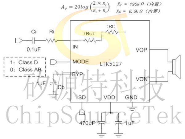
LTK5127 Typical application circuit

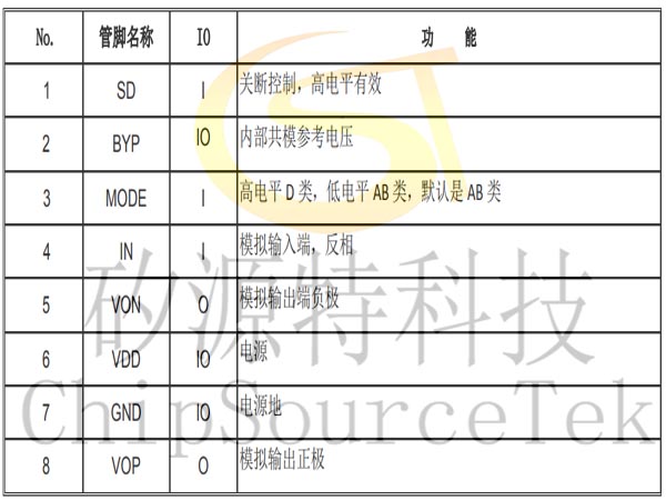
LTK5127 pin definition:
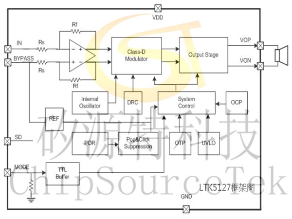
LTK5127 Schematic diagram Diagram:
LTK5127 Max rating (TA=25℃)
| Parameter name | symbol | Numerical value | unit |
| Operating voltage | Vcc | 6.0 | V |
| Storage temperature | Tstg | -65℃-150℃ | ℃ |
| Input voltage | -0.3 to +(0.3+ Vcc) | V | |
| Power consumption | PD | See note 1 | W |
| Junction temperature | 160℃ | ℃ |
LTK5127 Electrical parameters
LTK5127 CLASS D mode
1) Static electrical parameters of LTK5127
MODE=VDD, ClassD mode, VDD=5V, TA=25 ° C:
| signal | Parameter name | Test condition | Minimum value | Typical value | Maximum value | unit | |
| VDD | Supply voltage | 2.5 | 5 | 5.5 | V | ||
| IDD | Static supply current | MODE=VDD;VDD=5V,IO=0A | 2 | 5 | 8 | mA | |
| ISHDN | Turn-off current | VDD=2.5V 到 5.5V | 1 | uA | |||
| FSW | Oscillation frequency | VDD=2.5V 到 5.5V | 480 | kHz | |||
| Vos | Output offset voltage | VDD=5V,VIN=0V | 10 | mV | |||
| η | efficiency | THD+N=10%, f=1kHz,RL=2Ω; | 87 | % | |||
| THD+N=10%, f=1kHz,RL=4Ω; | 90 | ||||||
| OTP | Overtemperature protection | 155 | ℃ | ||||
| RDSON | Static on-resistance | IDS=0.5A VGS=5V | P_MOSFET | 180 | mΩ | ||
| N_MOSFET | 140 | ||||||
2) LTK5127 dynamic electrical parameters
MODE=VDD, ClassD mode, VDD=5V, TA=25 ° C:
| signal | Parameter name | Test condition | Minimum value | Typical value | Maximum value | unit | |
| Po | Output power | THD+N=10%, f=1kHz RL=4Ω; | VDD=5V | 2.9 | W | ||
| VDD=3.6V | 2.3 | ||||||
| VDD=3V | 1.3 | ||||||
| THD+N=1%, f=1kHz RL=4Ω; | VDD=5V | 2.5 | W | ||||
| VDD=3.6V | 1.6 | ||||||
| VDD=3V | 0.8 | ||||||
| THD+N=10%, f=1kHz RL=2Ω; | VDD=5V | 4.9 | 5.5 | W | |||
| VDD=3.6V | 3.2 | 3.5 | |||||
| VDD=3V | 2.3 | 2.6 | |||||
| THD+N=1%, f=1kHz RL=2Ω; | VDD=5V | 4.6 | 4.8 | W | |||
| VDD=3.6V | 2.8 | 3 | |||||
| VDD=3V | 1.4 | 1.5 | |||||
| THD+N | Total harmonic distortion plus noise | VDD=5V Po=0.6W, RL=8Ω | f=1kHz | 0.12 | % | ||
| VDD=3.6V Po=0.6W, RL=8Ω | 0.1 | ||||||
| VDD=5V Po=1W,RL=4Ω | f=1kHz | 0.12 | |||||
| VDD=3.6V Po=1W, RL=4Ω | 0.1 | ||||||
| PSRR | Power supply voltage rejection ratio | VDD=5V, VRIPPLE=200mVRMS, RL=8Ω, CB=2.2µF | 64 | dB | |||
| SNR | Signal-to-noise ratio | VDD=5V, Vorms=1V, Gv=20dB | 85 | dB | |||
LTK5127 CLASS AB mode (ESOP-8 package)
1) Static electrical parameters of LTK5127
MODE=GND, ClassAB mode, VDD=5V, TA=25℃ :
| signal | Parameter name | Test condition | Minimum value | Typical value | Maximum value | unit |
| VDD | Supply voltage | 2.5 | 5 | 5.5 | V | |
| IDD | Static supply current | VDD=5V,IO=0A | 6 | 10 | 14 | mA |
| ISHDN | Turn-off current | VDD=2.5V 到 5.5V | 1 | uA | ||
| Vos | Output offset voltage | VDD=5V,VIN=0V | 10 | mV | ||
| OTP | Overtemperature protection | 155 | ℃ |
2 LTK5127 Dynamic electrical parameters
MODE=GND, ClassAB mode, VDD=5V, TA=25℃ :
| signal | Parameter name | Test condition | Minimum value | Typical value | Maximum value | 单位 | |
| Po | Output power | THD+N=10%, f=1kHz RL=4Ω; | VDD=5V | 2.9 | W | ||
| VDD=3.6V | 2 | ||||||
| VDD=3V | 1.3 | ||||||
| THD+N=1%, f=1kHz RL=4Ω; | VDD=5V | 2.6 | W | ||||
| VDD=3.6V | 1.6 | ||||||
| VDD=3V | 0.8 | ||||||
| THD+N=10%, f=1kHz RL=2Ω; | VDD=5V | 4.9 | 5.5 | W | |||
| VDD=3.6V | 3.2 | 3.5 | |||||
| VDD=3V | 2.3 | 2.6 | |||||
| THD+N=1%, f=1kHz RL=2Ω; | VDD=5V | 4.5 | 4.6 | W | |||
| VDD=3.6V | 2.7 | 2.9 | |||||
| VDD=3V | 1.4 | 1.5 | |||||
| THD+N | Total harmonic distortion plus noise | VDD=5V Po=0.6W, RL=8Ω | f=1kHz | 0.18 | % | ||
| VDD=3.6V Po=0.6W, RL=8Ω | 0.15 | ||||||
| VDD=5V Po=1W,RL=4Ω | f=1kHz | 0.15 | |||||
| VDD=3.6V Po=1W, RL=4Ω | 0.12 | ||||||
| PSRR | Power supply voltage rejection ratio | VDD=5V, VRIPPLE=200mVRMS, RL=8Ω, CB=2.2µF | 69 | dB | |||
| SNR | Signal-to-noise ratio | VDD=5V, Vorms=1V, Gv=20dB | 82 | dB | |||

Please submit your basic information, send an email to Sales@ChipSourceTek.com, or call us at 13823761625 (same number as WeChat), and we will contact you as soon as possible!

WeChat Official Account

WeChat Service
 Email
Email QQ
QQ 13823761625
