
Products
Products

LTK8002D
LTK8002D is a high-voltage 4.2W, single channel AB class audio power amplifier with a working voltage of 2.5V-6V. It is connected by a BTL bridge and can provide an average output power of 4.2W with THD less than 10% to a 4Ω load under a 6V power supply voltage.
LTK8002D Description:
Input voltage range 2.5V-6V
Very few peripheral components
No need for coupling capacitors, bootstrap capacitors, and buffer networks
Excellent blasting sound suppression circuit
Ultra low noise floor, ultra-low distortion
10% THD+N,VDD=5V, Provide up to 3W output power under a 4Ω load
10% THD+N,VDD=6V, Provides up to 4.2W output power under a 4Ω load
Short circuit protection
Turn off current<1ua
LTK8002D Applications:
Bluetooth speaker, smart speaker
Portable game console, children's toys
Pull rod speakers, amplifiers MP3、
Various audio products
Portable game console, children's toys
Pull rod speakers, amplifiers MP3、
Various audio products
LTK8002D Package information:
| Chip model | Packaging type | Package Size |
| LTK8002D | SOP-8 |
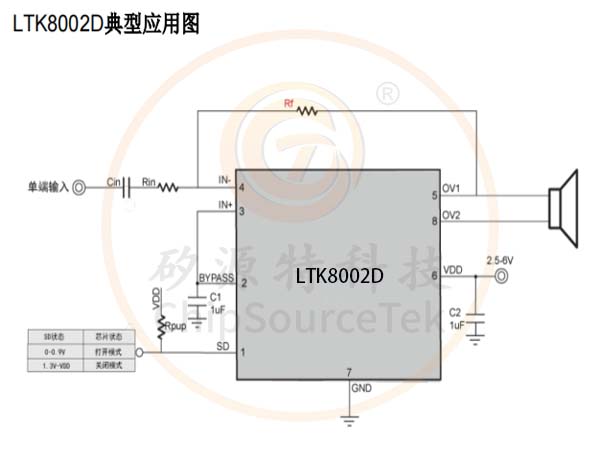
LTK8002D Typical Application:
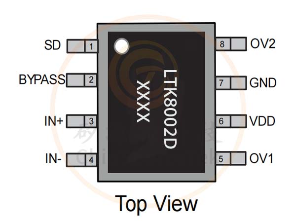
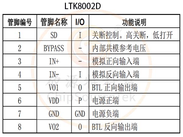
LTK8002D Pin description and definition:
LTK8002D Maximum limit value:
| Parameter | symbol | numerical value | unit |
| working voltage | Vcc | 6.0 | V |
| storage temperature | Tstg | -60℃-150℃ | ℃ |
| junction temperature | TJ | 160℃ | ℃ |

Please submit your basic information, send an email to Sales@ChipSourceTek.com, or call us at 13823761625 (same number as WeChat), and we will contact you as soon as possible!

WeChat Official Account

WeChat Service
 Email
Email QQ
QQ 13823761625
