
Products
LTK5328
Overview of LTK5328:
LTK5328 is a 2X8W built-in asynchronous boost audio power amplifier. The chip has PBTL function, adaptive boost, AGC anti distortion function, AB/D mode switching, adaptive and ultra-low noise floor, and ultra-low EMI. In PBTL mode, it can provide greater power to meet the needs of different customers. When the output amplitude is small, the adaptive boost circuit does not work, and the power amplifier is directly powered by the power supply. When the output is large, the boost circuit is automatically started internally, and the power amplifier is supplied with the boost voltage to achieve greater output power.
LTK5328 has 2 ALC modes to choose from, which can meet various needs and protect the speaker from overload and damage. The chip has AB/D switching function, which can reduce the interference of the amplifier on FM. The fully differential structure effectively improves the RF noise suppression of power amplifiers
LTK5328 Features:
Input voltage range 2.8V-5.5V
PBTL mode
Two types of automatic gain control (ALC)
Adaptive Boost
BOOST inductor current adjustable
No need for filter D-class amplifier, low static current, and low EMI
Ultra low noise floor, ultra-low distortion
THD+N=10%, VBAT=4.2V, provides up to 2X8W output power under 2 Ω+33uH load
THD+N=1%, VBAT=4.2V, provides up to 2X7.3W output power under 2 Ω+33uH load
PBTL mode: THD+N=10%, VBAT=4.2V, providing up to 7W output power under 4 Ω+15UH load
PBTL mode: THD+N=1%, VBAT=4.2V, provides up to 5.7W output power under 4 Ω+15UH load
Short circuit protection, under voltage protection, over temperature protection
Application of LTK5328:
Bluetooth speaker, smart speaker
Navigation device, portable game console
Pull rod speaker
Various audio products such as smart homes
LTK5328 Package:
| Chip model | Packaging type | Package Size |
| LTK5328 | ESOP-16 |
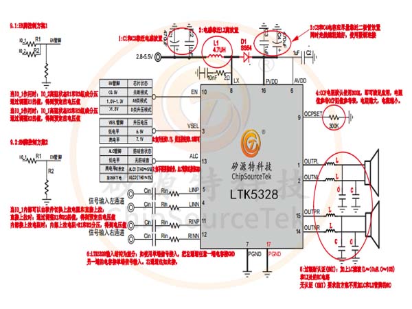
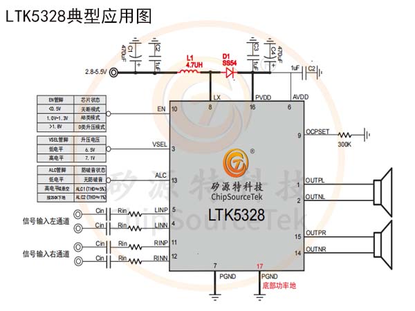
Typical application diagram of LTK5328:

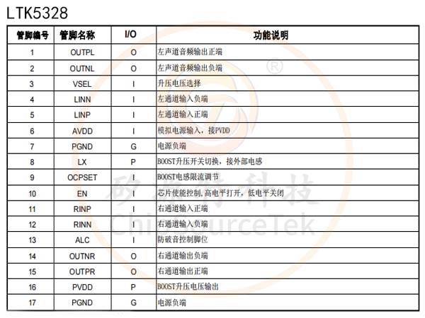
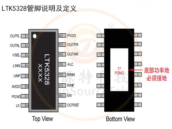
LTK5328 pin description and definition:


LTK5328 chip peripheral design and PCB layout, wiring suggestions:

The PVDD end uses a 470UF/16V plug-in capacitor and a 1UF ceramic capacitor in parallel, with the capacitor as close as possible to the PVDD pin. The VBAT end also uses a 470UF/16V plug-in capacitor and a 1UF ceramic capacitor in parallel, with the capacitor placed as close to the inductor as possible.
The BOOST boost inductor should be placed as close as possible to the LX pin of the chip, and the power supply pins (SW, PVDD) should be wired as thick as possible. It is best to use copper plating to connect the network. If a through-hole must be drilled in the wiring or copper plating, a porous connection should be used, and the inner diameter of the through-hole should be increased. It is not allowed to directly connect the power supply wiring through a single through-hole, because high current will cause a large voltage drop, which will have a significant impact on the output power. If there is a large impedance in the power supply, it may even affect the sound and cause stuttering.
The input capacitor (Cin) and input resistor (Rin) should be placed as close as possible to the pins of the power amplifier chip, and it is best to use a ground wrapping method for wiring, which can effectively suppress the noise of other signal coupling.
The bottom of LTK5328 is the chip power PGND pad, which must be grounded with good contact. It is recommended to use a large window with copper plating on the PCB at the bottom of the chip, which will greatly help with chip heat dissipation. The output pin of LTK5328 connected to the speaker should be as short as possible, and the wire width should be at least 0.5mm.
The bottom solder pads of the chip must be connected to the exposed copper GND part of the PCB. Due to a height error of 0.1mm (± 0.05mm) between the bottom of the chip and the chip pins, it is necessary to increase the thickness of the steel mesh appropriately during mounting. It is recommended to add about 0.1mm of filling material to the steel mesh at the bottom of the chip to increase the thickness of the solder paste, and regularly test and check whether the solder paste thickness can fully fit the bottom of the chip and the exposed copper part of the PCB.

Please submit your basic information, send an email to Sales@ChipSourceTek.com, or call us at 13823761625 (same number as WeChat), and we will contact you as soon as possible!

WeChat Official Account

WeChat Service
 Email
Email QQ
QQ 13823761625
